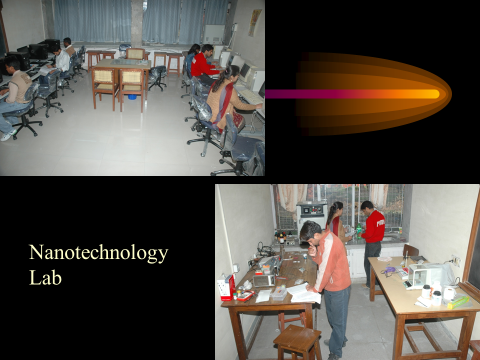
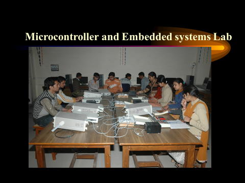
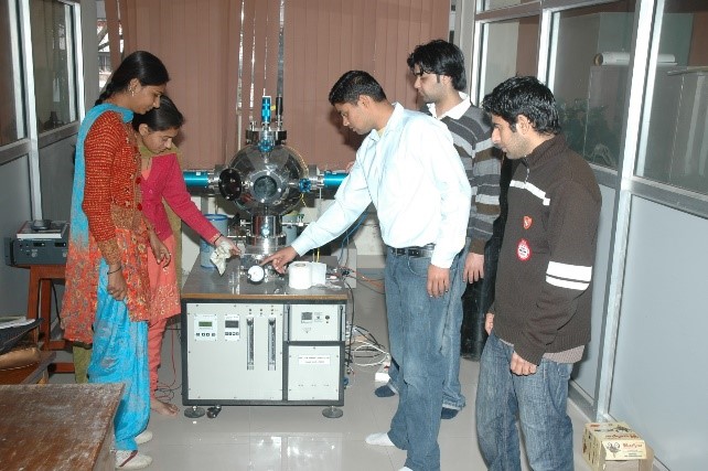
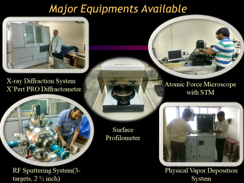
The Electronic Science Department was established in 1990 with the aim of generating specially trained manpower in the highly sophisticated field of Microelectronics, Integrated Circuit Design, Fabrication and Semiconductor Material Technology. This Department was established with funding from the then Department of Electronics (now, Ministry of Communication & Information Technology), Government of India, UGC and Haryana State Government. This Department is running a four semester M.Sc. course in Electronic Science since 1990. A M.Tech. Course in Microelectronics & VLSI Design was started in 2005 and a M.Tech. Course in Nano Science & Technology was started in 2008. All of these courses are job oriented with provision for project work and industrial training. There are laboratories for providing practical training to students in the areas of Device Fabrication, Thin Film Technology, Photo Lithography, Computer Aided Simulation and Design, Test and Measurement with modern equipment and facilities. The Department has established several advanced labs for teaching and research like VLSI Design Lab, Semiconductor Characteriza- tion Lab with advanced facilities like Atomic Force Microscope, X-Ray Diffraction, Spectrophotometer, Elipsometer, RF Magnetron Sputtering System. The Department has recently been selected to be a part of National Level Programme of NPMASS for MEMs Design.
DEPARTMENT VISION AND MISSION
VISION
To become a center of quality education ,research with innovation in the field of Electronic Science and be recognised at National and International Level for serving society
MISSION
To provide quality education to aspiring young minds for improving their scientific knowledge and technical skills in the area of Electronic Science. To produce socially committed trained professionals who can contribute effectively to the advancement of their organisation and society through scientific knowledge. To foster innovation in Electronic Science and Allied areas by collaboration with industry and other R&D organisations.
It gives me immense pleasure to introduce the Department of Electronic Science at Kurukshetra University, Kurukshetra. The Department was established in 1990 on the initiative of Department of Electronics (Govt of India) now Ministry of Electronics and Information Technology with an aim to generate trained manpower for the semiconductor and Microelectronics related industries. The Department is running an M.Sc. Programme in Electronic Science and an M.Tech. programme in Microelectronics and VLSI design.
These two programmes of two years duration each, with their advanced course structures, aim to provide high end technical knowledge to the students over a range of topics of immediate relevance in the rapidly growing areas of Semiconductor Devices, Electronic Circuits, Digital Design, VLSI Design, Electronic Communication, Embedded Systems etc. These courses along with other required basic courses give the students the required skills for working in industries related to these areas. As a part of the scheme of these programmes, students also undertake a project work of 6 months duration in a reputed Industry or R & D Institute/Lab in 4th semester of the program during Jan to June of the academic year. Due to the intense training, the students find placements readily in the various areas of Electronics. The department boasts of a large number of well-placed alumni in various multinational companies, premier institutes, research labs and as startup founders, who have been instrumental in helping the department in various aspects and the students to find good work place.
The Department faculty is also actively engaged in research in various areas. These areas include Semiconductor Materials and Devices, Nano materials and Devices, Micro-electromechanical Systems, Thin Film technology for IC processing, VLSI Design and Image Processing, Simulation and modelling of sub-micron devices for VLSI circuits, embedded system design, Electronic Communication etc. During the past five years, the faculty has published more than 50 research papers in journals of repute with more than 240 citations, impact factor of 1.4 – 4.5 and h-index ranging from 6-19. The faculty have completed 10 research projects from the outside funding agencies. The department has also been a part of the prestigious TEQIP programme during this time, which has helped the department to setup new research labs and to supplement the existing research activities with new sophisticated equipment.
This information brochure highlights some of the various achievements of the department, faculty and students during the last five years.